 Rationale
The Host chip has a 256 Mword flash memory and a 1Mword 16-bit SRAM. It has a 700 Mbps serial link to the Target chip.
I plan to use it for a variety of experiments, which I'll describe here. The goal is to port colorForth and OKAD to this platform and use it to design the next multi-computer chip.
Here are some pages of enduring interest:
If you have code you like, consider sharing it with GreenArrays.
I'm starting an ambitious new project on the Eval board. It will generate spin-off publishable code
Earlier I posted etherCode about random numbers. I've reposted it with corrections. My initial impression of randomness was refuted when I tried to produce normally-distributed numbers. I now use the high-order bits of the product, instead of the seed.
In order to compare 2 functions on the monitor, I've drawn one red and another green. A third can be blue. But there's another way. Alternate 2 frames:
Although you can plot more than one function if they're separated on the scan line, as I do with multiple scope traces, that gets difficult if they cross. Alternate frames fixes that. And with 3 colors you can display 6 arbitrary functions.
This is a good place to note that I plot functions with the ordinate horizontal at the top and the abscissa vertical at the left. That is, (0, 0) is at top left rather than the usual bottom left. This is enormously simpler, since single-valued functions require exactly one dot per scan line.
Some monitors can be rotated 90o counter-clockwise, which would restore normality. But this doesn't work if you want to superimpose text. I find it's easy to adjust to this new format, even though I've spent 50 years with the old.
And there's a discussion of video output available.
I inserted the DB-9 socket GreenArrays provides into J52 and soldered pins 2, 3, 4, 5 and 7. And soldered a 3-pin header to J54. And removed the jumpers
| J22 | J22 | |
| 1 | 2 | host 500.17 |
| 3 | 4 | port C |
Then connected 3 jumpers:
| J54 | J23 | |
| 1 | 10 | receive |
| 2 | 12 | send |
| J54 | J22 | |
| 3 | 4 | reset |
But the computer hasn't been idle. It's been running the clock display. Ran for 3 weeks before I joggled the board. Has run for another month since then. A reassuring test, that proves the chip is reliable and that I haven't disturbed it.
I have plans, as soon as I crawl out of my burrow.
First requirement is to know the day of the year. Recall that a c18 computer has 64 words of RAM. So everything must be done as simply and compactly as possible. Best I can do is a 12-entry table of the 0th day of each month. Although I can neatly calculate the days in each month, it take more than 12 words. And I can ignore leap year for the next 2 years.
The longitude of Incline Village is 119:43, 17 minutes of arc east of the 120:00 meridian. So Mean Solar Time is 68 seconds from PST. The Equation of Time yields Apparent Solar Time which can be 15 minutes off. But it is quite complicated. The simplest approximation I've found requires the sine function. Would interpolating a table be smaller?
Then I need to know the length of a day, or equivalently sunrise and sunset. This is another calculation to be simplified.
So there's a way to go. Why am I doing this? Out of disgust with Daylight Savings Time. I get up at dawn and don't care what Washington wants to call it. The cost and confusion of changing clocks twice a year is ridiculous. Especially when the dates of doing so also change. I'll live on local time.
For example, classic Forth has a double-length version of 2* called D2* . I would like to call the colorForth analog 2*d .
The rationale is that the operation is most important, with the modifier basically a subscript. This groups all versions of an operation together in an alphabetical listing.
If the small, but growing, community of colorForth users agree to this convention, it can make life a little easier.
As another example, John named the operators sd@ and sd! to fetch/store from/to SDRAM. I'd like to call those @r and !r indicating fetch/store from/to (external) RAM. It's shorter and somewhat more generic.
Comments welcome.
The problem getting it working was simply sloppiness. Node 127 had to be started by 117. Registers had to point to the correct port. This was a rework of the previous layout and I failed to change things correctly. On the other hand, it has the most complex cooperation I've ever attempted.
So, onward. Next I want to sample Vss and Vdd 768 times and display them. This will show power supply variations? Requires SDRAM which I now have.
For example, node 27 talks to all its neighbors: 26, 28, 37 and 17. Their RAM is loaded according to a path in the order 37, 26, 27, 28 and 17. They must not be started until their RAM is loaded. Sounds simple, but now I'm working with 30 nodes on 2 chips. It will only get worse since I've 360 nodes on 9 chips.
John has been here and sorted out the SDRAM interface. The wiring was different than expected, so control patterns changed. Sadly, Haypress Creek can only access 16 mega-words per chip. The potential of 32 will have to await the new board. But I can read/write SDRAM and that opens up new applications.
I have the 48 characters for colorForth designed. It takes a node (124) to store their descriptors: one word for each 3x6-pixel array. I can display red, green and yellow words. Those needing blue are pending. My plan is to store some colorForth blocks in DRAM and display them. This will be the first interpreter. Soon as I get one I'll post it.
I've learned a bunch about choosing paths and starting nodes. I moved from sampling by node 137 to node 139. Now I've moved to node 39, with a long path into chip 1 to node 127. Want to explore the noise environment of chip 0, which has no other activity.
All nodes default to listening to their neighbors/pins. The first to break this symmetry takes charge. Apart from the boot node (33) that's nodes 132 (10 MHz resonator) and 39 (sampling). They spontaneously write to a neighbor, whereas everyone else reads until awakened. The strategy is to make sure no one writes inappropriately. Then you can start nodes as they're loaded.
It's obvious that the distribution is bi-modal. There are 2 Gaussian peaks where there should be one. Don't know why, but it's saying something profound about the internal environment of the chip.
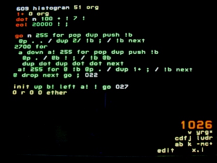
That histogram is an interesting application. Node 17 accepts samples from 37 via 27. It computes a 50-point histogram from minimum and maximum values using */ . (Remember that */ requires a negative divisor; I forgot.) It passes each value to node 18, which has 50 RAM locations to store them.
One sample is taken each video frame, during vertical retrace when nothing is happening. The histogram is passed back from node 18 to 37, via 17 and 27, to be displayed. It gradually builds up as samples accumulate and is interesting to watch.
A wire node is one that passes data from one neighbor to another. It might do other work, but passing data is important.
There are many ways of doing this. Many more than I ever anticipated. There is no right way; optimal coding depends upon the application. So I've prepared a white paper that discusses it.
I added - and . to the displayable characters. I'm using */ and double-precision arithmetic. Good progress.
All in all I'm very pleased. This chip can monitor its own temperature, providing it has a time reference (the ceramic resonator). Its voltage is fixed at 1.8 V by a regulator, otherwise it could monitor that. My next step is to monitor the Li-ion battery (3.6 V).
I modified the memory display with a green plot of its readings: Received sqrt code from John. Have to study it. Will be part of my Arithmetic white paper, due here soon.
Warning to c18 coders; this just stung me. If you add some words to your code, subsequent addresses may change differently than you expect. This is due to slot 2 jumps, which are limited to an absolute 3-bit page. Adjusting code may move it into or out of such a page.
134a9 at the bottom is the fill pattern for empty memory. It's a jump to somewhere safe to try to catch bad code.
I just learned something about the jitter on the display. It increases as the scan line progresses. Which indicates it comes from executing instructions, not the sync pulse. I now generate 2 pulses for each line: This jibes with Greg's observation of some 5% variation in instruction timing. That must be due to voltage fluctuations, in spite of our on-chip capacitance. Larger than I had expected. So our timing is not stable enough for video. Need a pixel clock.
Was a nice challenge. Relaying that sync message taught me a lot: I'm stoked. This clears the way for more ambitious applications.
I needed /mod and devised nice code for it I'm working on a clock display: hours and minutes. Driven from the 10MHz resonator. To do this I have to address the issue of multiple applications within IDE. I've refactored some code and reorganized so that each application has its own script. That's working. Now to relay the sync message to the analog nodes.
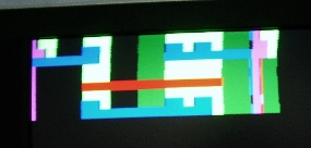
Colors did not come out right in the picture. White should be green for diffusion; green and blue should be darker. Magenta needs to be made white for metal-2. At least I didn't get a scroll bar.
So this is the current state-of-my-art. 9 nodes cooperate to produce the image on a line-by-line basis. A single instruction can cause a visible delay. Nanoseconds count. The code is optimized with instructions executed from ports. Fun to code; difficult to perfect.
I fetched my tripod from the cabin, so future screen shots will be better.
Got the ceramic resonator working nicely. Strategy is threefold: Note on the trace the pump pulse followed by 9 counts (actually 10; pretty close). That is repeated 20 times to obtain 50 KHz timing. The duty cycle of pumping can vary from 5% to 100% and controls the amplitude of the sine wave (1.7 V), which gradually decreases. Smaller duty cycle, less power consumed, less RFI. The starting sequence can be as few a 8 cycles.
The resonator is less precise than a crystal, costs less and is easier to start. This non-linear drive requires only 1 pin and pins are a valuable resource. It does require 1 node, but nodes are cheap and plentiful. And the node can do other tasks, such as provide 50KHz and 60Hz signals.
Code is optimized by pre-filling the stack with numbers: Dividing it by 200 would provide 50 KHz for a jitter-free horizontal sync.
I transitioned to a floppy Greg gave me some time ago. It has OKAD removed, so is suitable for distribution. Has the g18 compiler and S40 IDE. It startled me that booting and saving were so fast. There are only 7 cylinders of compressed source. Nice.
I'm using nodes 36, 37, 38, 39, 26, 27, 28, 29 and 17: Quite a puzzle organizing these nodes: But timing is crucial. I had trouble with a 2-port write because one neighbor read earlier than the other. He cleared the write and the other neighbor had nothing to read, and hung.
Such hanging is a joy. It doesn't destroy the group effort, just a portion of the output. Which is a precise diagnostic of the problem.
IDE is working marvelously. There are improvements to make that will simplify operations. But complexity has to be conserved. And I want to start using Flash and DRAM, if only to speed interaction - 115,200 baud is awfully slow.
The basic timing mechanism is the unext loop. It allows timing to 2 ns resolution. Much better than your generic 15ns, 1024-pixel scan line using a pixel clock. Still to be determined if jitter will allow such precision.
Speaking of which, I just realized that there is no de-coupling capacitor on analog power. Looks like there should be.
A very pleasant programming environment results when errors are localized. There's more to be gained: If I'm programming node 29, I only need to compile and reboot node 29. Presently, I'm re-booting the entire board. When I get time, I'll reorganize the paths and procedures. It's a familiar, unfortunate situation: I haven't the time to invest in efficiency; but I have the time to waste being inefficient.
But I'm making progress: I have a row of 9 tiles, with well, diffusion and metal-1: horizontal and contacts. Each tile occupies 69 scan lines and 69 pixels, in keeping with the .69um tile size. The image is not correct, with several artifacts, but it's getting there. Biggest challenge is making colors opaque, within the constraints of time and code size.
I don't know how to do this. I'm just trying what occurs to me and seeing how it works. One strategy that seems inevitable is to recompute. I had expected that the blue node would inform the green node about masking. But it seems simpler to let the green node recompute the masking. It has the information and the time (if blue can compute it, so can green).
The simple solution is to designate node 01.27 as 127. This only required some 100 mod phrases.
So now I have the first tiles displayed: 2 tiles, one over substrate and one over well. I'm working to implement this tile descriptor: .4 4433 3222 11pp pddw
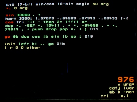
The cosine is integrated with a simple difference equation:
The starting values are both 256 (values are divided by 4 for display). This appropriately starts the integration at the peak of the cosine and establishes the amplitude. The frequency can be decreased by moving the multiplier closer to 2.
It was fun working out the cosine. First attempts put red dots all over the screen. Then I had the frequency too high; multiplier too far from 2. Then I had to get the right amplitude. That's easier with the cosine than the sine. It seems the function display is not quite consistent with the grid. I'll eventually correct that.
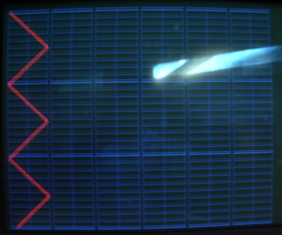
Then I superimposed a red triangle wave running vertically, ala chart recorder. That's much simpler than horizontal because each scan line has a single red pixel.
Note that this display is re-generated for every frame. There is no image stored, just a colorForth description. This assures any changes will be re-displayed at 60 Hz. The triangle wave does indeed scroll against the background grid.
Here 'tis. Another kind of jitter because of the long exposure without tripod. You can see 6 slots for traces, 128 pixels per trace. Triangle wave in first slot. 3 ns vertically; 100ps ticks with 1ns brightened.
I'll show you code sometime. The grid took 56 words of RAM. It also took all 9 words of return stack, being highly nested.
Video requires a horizontal sync pulse every 20 us. This is 1.8 V through 75 Ohms for 24 mA. The 3 colors are .7 V, same load, for 9 mA each. At a different time than sync. So the power supply needs to accomodate 25 mA sub-uS pulses. Working on it.
At power-up, the b register contains the address of IOCS. This is very convenient and seemed worth the 10 transistors it cost. One tends to expect this and not bother setting b. But after IDE traverses a node, b has been changed. It now points to the output port, while register a points to the input. Although these could be reset, that doesn't seem worth-while since the correct values depend upon the next activity.
So, at start-up of most nodes by IDE, b should be set. For edge nodes doing I/O, this would probably be: io b! .
Jitter is worse. If I disconnect the serial cable, it gets a little better. I'll take a picture, but now I'm off to the cabin.
I removed the 2nd serial interface, which is no longer necessary, and that reduced the noise level. So maybe it's external to Haypress Creek. I turned off all my computers. Didn't help. But then the office is full of servers.
Now programming nodes 36 and 37 to generate red and green.
Yesterday Greg brought in a second PC and serial cable. We hooked it up to 01.33 and ran IDE on chip 01. First we had me on chip 00 and Greg on 01 and looked at the communication nodes 00.19 and 01.10. They weren't talking. I finally found the blunder in the handshake code (missing dup). Then everything started working.
I extended my 00 path into 01 and at one point we were both hooked to 01.11. This is absolutely amazing! Two programmers, 2 development environments, debugging the same computer. With 19 other computers assisting. Consider the potential for shared development of the 360 Haypress Creek computers.
Presently I'm generating a 50 MHz square wave on 01.38.17. The code is
The key to understanding IDE is the path: a list of nodes starting at 00.33 for my set-up. I'm using 00.23 13 3 4 14 24 25 26 27 28 29 (19 01.10) 11 12 13 14 15 16 17 18 28 38. This gets me to 01.38 which I'll use as video sync generator. Nodes 19 and 10 are a serial connection between chips and don't actually appear in the path.
If I say 11 hook I can examine node 01.11. If I say 12 hook I should be able to examine node 01.12, but that doesn't work.
What I learned today is that I must detour through nodes 13 3 4 and 14. That's in order to dump the stack from 01.11. Stack entries are burst back along the path to be sent to the PC at 115,200 baud. The path must be long enough to back up 10 entries. This will be relieved when I get a handshake between nodes 00.19 and 01.10.
In following the path, each node has 2 sides: input from its predecessor and output to its successor. 0 side and 1 side, respectively. For example, node 13 receives input via its up port from node 23 and sends output via its down port to node 3. Normally 1 side of a node is the same as 0 side of its successor.
This fails between nodes 29 and 11. 29 goes up to 19, across to 01.10 then right to 11. So 1 side of 29 is up; but 0 side of 01.10 is right. Path code must take this into account, but apparantly doesn't quite.
The synchronous communication required to boot 01 is mysterious. It derives from TPL's development board which included an On-Spec USB chip. That chip was specially programmed for TPL, but could not meet the SEAforth spec. So we ended up with an unsatisfactory interface, difficult for the PC and difficult for S40. That legacy persists on Haypress Creek. It will not for GreenArrays' chips.
Now to test the new communication protocol.
Turns out that the clock line goes high for wake-up. Thereafter, each edge clocks a bit. Unfortunately, that leaves the clock line high. Which makes it hard to tristate the lines so that 01 can send. So next I'll retrofit the 1-wire protocol pioneered by GA4.
Meanwhile, Greg is implementing an IDE path suitable for 01.
I've moved the path to 33, 23, 24, 25, 26, 27, 28, 29, 19. Telling node 29 to reset chip 01, then loading 19 with synchronous serial send code, I'm ready to boot 01.10.
Meanwhile, here is the poster for S40 with all the pinouts. But only some are brought to vias on Haypress Creek.
The async node is 33. Nodes are numbered 00 - 39 from lower left, so this is top center. Chips are 00 - 33 from lower left. So this is node 00.33. For node 33, IOCS bit 17 is serial in, bits 0,1 are serial out. So that input bit can be designated 00.33.17.
Node 33's ROM contains the serial boot code and it boots looking for a start bit. The PC sends it bytes at 115,200 baud. Starting with the IDE code which includes a target node and the path to get there. I'm going to target node 3 via nodes 23, 13.
Ok! That's working. I compiled code for node 3 that toggles bit 0 of the data bus. To see it I had to wheel up our Tektronix 2465B scope. That's always a problem: To verify your code's working you have to do something visible. Blinking leds, scope traces, audio or video out.
I was going to generate video. But the D/As are not brought out to pins for chip 00. So I'll have to get into chip 01 before I can do that.
Greg has programmed an Interactive Development Environment (IDE) in native colorForth. That's what I'll be using. A slightly different version works with Windows colorForth. It's a rich environment that I'll have to learn to exploit. I'll lead you thru it over the next days.
So far I've learned to type: At this point, typing 123 lit will put 123 on node 23's stack. Typing dup will cause node 23 to execute a dup instruction. And you see this behavior on the panel display.
Now I've got to write some code for some node to execute.
Typing 0 64 23 boot 0 call will load the code compiled for node 23 (64 words starting at 0) into RAM for the current node and start executing at 0.
Tomorrow. Now I've got to go home and await my mattress.
It is extremely useful to control Reset from the PC during development. That will become unimportant once I have code that reprograms the nodes while they're running.
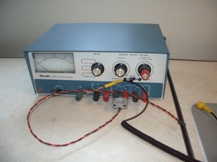
The one feature I'd really like is a milli-Amp meter. This one measures Amps up to 20. A sign of its age.
It's providing 1.8 V on Supply A with some huge current capability. I've long lost the user's manual. As long as it gives me 500 mA, I'm fine for Haypress Creek. Hey DARPA, here's your 1 W supercomputer!
The red/black power cord has the right connector for the Haypress Creek board. The board has a lot of vias to which wires can be soldered. 4 of those are connected to an RS232 interface board. It provides serial input/output and reset from a PC. Soon as Greg gets me a cable, I'm good to go. Should be fun.7 October 12:00 Wednesday
Hoorah! I finally got A/D sampling from node 039 working. But no change from node 139. I have a narrow histogram peak with several subsidiary peaks. A distribution that can't be averaged.
5 October 3:00 Monday
Great progress over the last weeks, but little to report. Working with the chips requires routing communication and control correctly. This I haven't mastered.
22 September 10:00 Tuesday morning
Been working on sampling A/D. Fascinating problem. I can get 10 bits easy. But I want 18. The histogram provides ground truth: the longer I sample, the wider the distribution. This suggests low frequency voltage variation. At 4000 counts (500 ns) I get a histogram peak 3 counts wide.
I've been reading the A/D as it measures Vss. This will vary with temperature, but the scatter has been large. The image shows a green histogram of that scatter: smallest value at top, largest at bottom.
 14 September Monday afternoon
5 September Saturday afternoon
Yesterday I was trying to get SDRAM to work. In order for node 25 to talk to node 23, node 24 had to become a wire node.
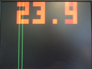
Here's the latest display, this time of chip temperature (Celsius) The left green line is a reference, the right the A/D counts averaged over the previous frame. The numeric display has been tenatively calibrated. The low digit is flickering between 4 and 5.
 2 September Wednesday morning
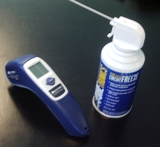 I bought an infrared thermometer to aid in calibration. A Kintrex that measures from -60 to 500 Celsius. I have a can of Circuit Freeze that can chill to -50 C. So far I've been to -3. Squirt the chip and the green line zooms to the right (circuits get faster as temperature drops) then drifts back.
29 August Saturday afternoon
Yesterday morning I got node 137's A/D working. Just as advertised in the spec sheet.
The goal is the examine repeatability and noise. And to see how much I can average to reduce noise. And to calibrate voltage tracking. More work to do.
27 August Thursday morning
This jitter is very interesting. It amounts to only a 1% timing variation, but it's not random. Most telling is that of 50 identical scan lines, some suffer quantized delays; but never 2 adjacent lines. During that time all computers are repeating the same code. Indeed the entire environment is identical for each line. So any induced voltage variation would be repeated. Most puzzling.
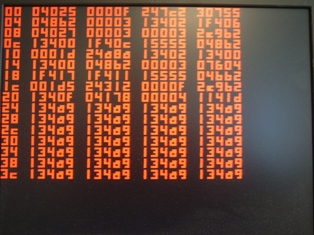 I can now display a hex memory dump, 64 words from node 127. This will be useful in testing DRAM. I did something like this a year ago on the S24 chip. So to call it progress is dubious.
Whoops. I posted the clock display on the other blog. Here it is again.
 26 August Wednesday afternoon
The display is now rock solid at the left edge. Gradually deteriorates as timing variations accumulate.
20 August Thursday afternoon
Ok. I have a clock running. Counting 60ths of seconds, displaying minutes. Camera needs batteries, but I'll post a picture.
5 nodes do the work with 4 more connecting them
Jitter is much reduced but still present. Can see it on the oscilloscope. It might be amplitude noise coupling to phase. Next step is to improve the wiring.
/mod a! 3ffff for dup a . + -if drop pop - ; then next ;
It takes 2 arguments: a positive number and a (negative) divisor. Returns modulus and quotient by repeated subtraction. For example
1234 -100 /mod
returns 34 12. Below these results, the stack is garbage. I particularly like the way counting down an index can produce a increasing quotient. I originally called this word digit and it took a while to realize that it was identical to /mod.
15 August Saturday morning
Been busy with layout for coming chip submission. GA4 has several nice enhancements and GA144 gets its first try.
I've been recoding the layout display. Now have an inverter displayed reasonably well. Still some geometric corrections to make. But it's time to move on. Next I'll construct a 3-ring oscillator.
 6 August Thursday morning
3 August Monday morning
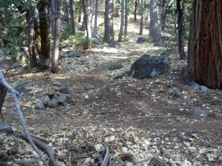
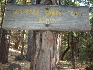
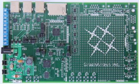
Here's the Haypress Creek Trail sign; picture taken on my Sunday hike. And the trail as it starts from the Pacific Crest Trail. It's the icon for the Haypress Creek board.
(The picture is small because I can't hold the camera steady enough for the long exposure.)
 31 July Friday morning
You detect going high/low by fetching from the up port after selecting a high/low level. Node will sleep till the transition occurs, then synchronize accurately.
The various modes - start, pump, count - each select from these and drop those that are irrelevant. The 8 numbers appear repeatedly from the 8-deep circular portion of the stack.
30 July Thursday morning
Yesterday I got a 10Mhz ceramic resonator to oscillate. I connected it between pin 01.32.17 and ground. Then switched it up, tristate, down, tristate at 10 MHz. Today I plan to examine how it starts and optimize that. Then let it free run, waking node 32 on edges and supplying minimum drive.
29 July Wednesday morning
I'm displaying an inverter, sort of. A 9 x 3 array of tiles that shows well, diffusion, poly and metal-1. Doing so has been an enriching experience. Now that I know what works, I'll start over and do it right.
Multi-port reads and writes are an invaluable tool. For example, a 2-port address that is used to read and write. This depends upon one neighbor who reads and another who writes. So context determines who does what.
Yesterday I programmed color bars. I needed to calibrate the display better. I learned a few things: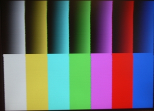 28 July Tuesday morning
I can't time a universal pixel. It depends on the image being generated: fast pixels, slow pixels, some of each. Best example is the color bars and color ramps. They use different timing.
24 July Friday morning
I've just realized a very nice advantage of multiple computers. I'm programming the 2 blue nodes: one that puts out video from run-length encoded commands; and another that generates the runs from the tiles. I make my usual number of mistakes, some of them fatal. But that only affects the blue video. Green and red are running independently and continue happily.
23 July Thursday morning
Solved an amusing problem with IDE paths. A path in chip 00 transitions to chip 01 via nodes 29 and 11 and then continues. My path 0 included node 27 in both chips. When I tried to hook 01.27 I got 00.27.
where metal# and poly mark contact, vertical, horizontal. First I'll lay out an inverter.
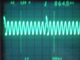
Here's the same grid with a 5GHz cosine trace in red. The green trace is advanced 120 degrees. They represent 2 outputs from a 3-ring oscillator.
 22 July Wednesday morning
cos over - over 2* dup 2/ 2/ 2/ 2/ 2/ 2/ 2/ - . + . + 2 . + ;
The 2 previous values are on the stack. A new one is calculated and the oldest falls off the stack eventually. The previous value is multiplied by almost 2; actually 1/128 less. And the oldest value subtracted. Adding 2 corrects for using ones complements instead of negates.
22 July Wednesday early morning
Yesterday I played with the video. I put up a 900x700 grid with lines every 10 pixels with every 100 intensified. I did it in yellow, then transitioned to blue.
 I expect all my displays will be dynamic in this sense. That makes them unsuitable for a snapshot. Still, I will photograph the screen occassionally. Not for this grid, tho. Today I plan to format the OKAD Hardsim display.
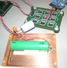
The jitter problem is due to the power supply. My venerable HeathKit is not up to this task. Greg has an HP supply that is much better: jitter reduced an order of magnitude. Glen has combined a tiny voltage regulator with a Li-ion battery that might be even better. Here it is.
 20 July Monday afternoon
![]() So here's the display of my colorForth logo. The colors are transparent instead of opaque, but I'm getting there. Looking closely at the left edge you can see the remaining jitter. There's a flash spot and the scroll bar, but you get the idea.
So here's the display of my colorForth logo. The colors are transparent instead of opaque, but I'm getting there. Looking closely at the left edge you can see the remaining jitter. There's a flash spot and the scroll bar, but you get the idea.
20 July Monday morning
I want to mention the problem that slowed me down last week. Greg reminded me of this characteristic of the IDE:
16 July Thursday afternoon
After sorting out some path problems, I've got a white rectangle. Nodes 36, 37, 38 and 39 are generating red, green, sync and blue.
16 July Thursday morning
Yesterday I got a blue rectangle displayed on my Mitsubishi monitor. Node 01.38 generates the sync and 39 the color. Unfortunately, the image is very jittery. Trying to chase that down.
14 July Tuesday morning
Ok! I've communication with and signals from 01.38.
begin over over !b !b end
That's a 2-instruction loop producing at 3:2 duty cycle.
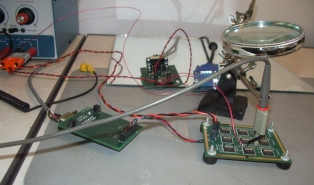 To see the squareness of the wave, I had to use the short signal and ground scope probes. Haypress Creek is nicely supplied with ground vias. With a 3rd hand, probing vias is very convienient. Probing signals not brought to vias is not practical. Such as the 19-10 serial trace. You can see the 2nd serial board in the back.
13 July Monday morning
Still hammering away at getting IDE into chip 01. I can access node 01.11 but not node 01.12.
8 July Wednesday morning
Somehow I lost the ability to talk to chip 01. I have just recovered it. 00.19 boots 01.10 which tells 01.20 to raise pins 6 and 7. Ok!
5 July Sunday morning
Ok! After Dean reminded Greg what the actual synchronous protocol was, I have successfully booted chip 01.
4 July Saturday afternoon
Click these Haypress Creek photos for high-resolution. 
3 July Friday evening
So I moved the video to node 03. Sync on D00, green on D01. I've generated the frame sync but the monitor doesn't like it. When it works, this will give me the 8 primary colors. To be continued . . .
3 July Friday morning
Had to change last night's entry a little. If this were a real tutorial I'd be better organized.
2 July Thursday evening
Ok! My Haypress Creek board is connected, powered and running. I'm using Supply B on the power supply 'cause I could set 1.800 V more easily.
This sequence of actions will be scripted when it stabilizes.
2 July Thursday afternoon
I have the RS232 cable. The pins used on the DB9 connector are:
Request to send is connected to Reset on Chip 00. Reset for the other chips are daisy-chained from 00. I'll report the order when I find it out.
This is my venerable HeathKit power supply. It works fine and I've used it with all my chips, from Novix and ShBoom to S24. I've tried to replace it with a newer model, but can't find anything comparable.
 2009 30 June Tuesday morning