SDI flash
The SST25WF080 is flash memory with an SPI interface. GA144 ROM code can boot from it. It provides 1MB of memory, which I access as 512KW.
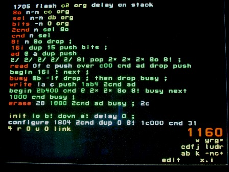
This is code I've used to read/write the memory. It's been a while so my explanation may be weak.
The code has no paging, so an 18-bit address can access only 256 KW. But it looks like it's restricted to the first 128 KW.
8o
Code in ROM to send 8 bits, left-justified in an 18-bit word. It expects a timing delay (0) in S, so there can only be a single output word.
sel
Code in ROM to raise and lower chip enable. This identifies the following input as a command.
bits
Code in ROM to return n right-justified bits.
2cmd
Send 2 8-bit commands, left-justified in an 18-bit word.
cmd
Send 1 8-bit command, left-justified in an 18-bit word.
8!
Send 8 left-justified bits and discard the remainder.
16i
Receive 16 bits. This code is intended to transfer data to 16-bit SRAM. From there it can be unpacked into 18-bit words if appropriate.
ad
- Fetch an 18-bit word address. In this case from down
- Flash expects a 24-bit byte address
- Send high-order 3 bits (Don't understand propagation of sign bit. Probably never tested beyond 17 bits)
- Send middle 8 bits
- Send low-order 8 bits (last bit 0)
read
Don't understand how push over drop are arranged. For debugging?
- Retrieve delay
- Send read command
- Send address
- Push count
- Read and store (to down) 16-bit words
busy
Fetch flash status until it becomes negative.
write
- Push count
- Send 2-byte write-enable command
- Send address
- For each word
- Send write command
- Fetch word (from down)
- Left-justify
- Send 16 bits
- Wait while busy
- Send end-write command
- Wait while busy
erase
Flash must be erased before it can be written, in 4K chunks
- Send 2-byte erase command
- Send address (multiple of 2K words)
- Wait while busy
init
- Set address registers
- Leave delay (0) on stack
- Don't understand why configuration is commented out. Perhaps it's done in ROM
- 3 commands establish no protection and enable busy