16-bit SRAM
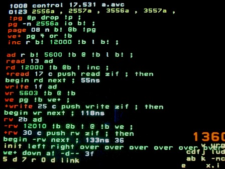
This code in block 1360 is loaded into node 008 of the host chip. It provides access to SRAM, aided by nodes 007 (left) which has 18 data pins and 009 (right) which has 18 address pins. 008 has 4 control pins.
There are entry points for random and sequential read/write and read/modify/write. The challenge is to optimize sequential read, since reading is more common than writing. The 3 nodes cooperate to do so. For sequential
- read 55 ns
- write 118 ns
- read/modify/write depends upon modify
Paging
The CY62167EV18 SRAM chip has 20 address pins to access 1 MW of 16-bit wide memory. The GA144 has 18 address pins accessing a page of 262,144 words and 2 others that select 1 of 4 pages.
The first 4 words of 008 RAM specify select bits for the 4 pages
- Page bit in bit 16
- Page bit in 4
- Write-enable low in 2
- Chip-select low in 0 (unchanged)
Register b normally holds left. Temporarily right or io.
!pg
- Store page bits into the parameter word of pg
pg
- Leave page bits on stack
- Put io into b
page
- Take a page number
- Fetch the indicated word
- Store with !pg
- Bits are set to enable writing (to optimize write). Fall into +we to turn them off
- Address increment irrelevant
we+
- Get page select
- Turn off write enable (io2)
- Fall into inc, partly to restore left
inc
- Set b to right
The stack is filled with alternate left and right entries by init for ease in switching between nodes 007 and 009. Comments l and r indicate which is on top.
- 009 keeps the current SRAM address on its stack.
12000 says increment this, anticipating the next access
- Reset b to left
ad
Passes an address to 009
- Set right
- Fetch address from down, the input port
- Pass to 009 with 5600
- Reset left
read
Entry point for random read
rd
Does the work of reading
- Tell 007 to read current word. Timing is controlled by 007
- Relay to up
- Increment address
+read
Sequential read entry point
- Push 0-based count
- Call read to get first word
- Decrement count (zif)
- Repeatedly call rd
write
Entry point for random write
wr
Does the work of writing
- Tell 007 to write current word.
- Relay from up
- Fall into we
we
- call pg
- Set write-enable
- Jump to we+ to reset write-enable and increment address
+write
Sequential write entry point
- Push 0-based count
- Call write to write first word
- Decrement count (zif)
- Repeatedly call wr
rw
Random read/write entry point
- Get address
- Fall into -rw
-rw
Does the work of read/write
- Tell 007 to read a word
- Send it for modification
- Fetch modified word
- Write it back with we
+rw
Sequential read/write entry point
- Push count
- Call rw for first word
- And -rw for rest
init
- Initialize stack to alternating left, right with right on top
- Call we+ to set page bits to read and b to left
- Set a to down and call the down port for instructions